

PV Output Optocouplers
Features
Polaris Semiconductor’s photovoltaic output optocoupler is the core technology driving our innovative products. It provides unprecedented power transfer efficiency in a very small footprint. The devices employ our proprietary GaAs-based optocoupler technology, achieving high current transfer ratio and power transfer efficiency over a wide range of drive currents. These optocouplers are radiation tolerant by design. This technology will enable new power architectures in demanding applications and are suitable for low voltage applications including DC voltage conversion, high-current MOSFET gate-driving, and low-voltage isolated signal transmission.
Core Values
Breaking Efficiency Barriers
Polaris Semiconductor optocouplers achieve unprecedented power transfer efficiency, surpassing market alternatives by more than 25 times. This revolutionary performance enables new possibilities in power management, gate driving, and low-voltage isolated signal transmission. Our innovative technology fundamentally transforms optocoupler capabilities, opening doors to previously impossible circuit designs.
Enabling Footprint Savings
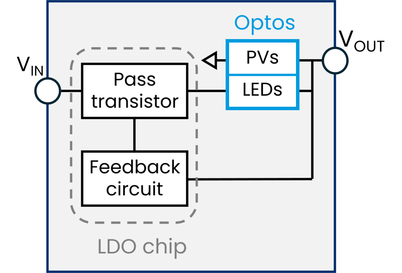
Our optocouplers deliver exceptional volume efficiency through our unique monolithic architecture, with a compact 16mm² QFN footprint and 0.8mm height. These versatile devices seamlessly integrate with our enhanced linear regulators — replacing conventional switching regulators — while also eliminating the need for bootstrap circuits in high-side MOSFET gate driving. The result is dramatically reduced board space and simplified circuit design with fewer components.
Environmental Resilience
Through advanced engineering, our optocouplers deliver superior performance in the most challenging environments. The radiation-hardened design ensures reliable operation under both ionizing and non-ionizing radiation conditions, while maintaining consistent performance across extreme temperature ranges. This robust environmental tolerance makes our devices the definitive choice for demanding terrestrial, aviation, and space applications.

Product Summary
We currently offer one family of photovoltaic output optocouplers. Key performance attributes are summarized in the table. The product page can be accessed by clicking on the device family below. Full datasheets are available upon request. All products are also available on evaluation boards.
If you don’t see a product that suits your application, get in touch as we also offer custom designs, including multi-optocoupler packages.
| Device Family | VLED Range |
ILED Range |
Typical VPV |
Peak η1 |
Peak IPV/ILED |
|---|---|---|---|---|---|
| OC1D | 1.2-1.7 V | 0.5-500 mA | 1.0-1.2 V | 52% | 74% |
| 1 Efficiency is defined as the power out of the photovoltaic divided by the power into the LED |
|||||

Tech: Monolithic GaAs Device
40V Junction Isolation
Applications
Enhanced Linear Regulators
High-Side Gate Driving
Isolated Signal Transmission
Understanding our Optocoupler Products
You can contact us with your desired specifications, or explore the details below better understand the capabilities of our optocouplers.

Revolutionary Architcture
Unlike traditional optocouplers that combine discrete components for high-voltage isolation, our GaAs-based devices are epitaxially-grown in a single monolithic structure. This fundamental architectural difference enables unprecedented power and current transfer efficiency, while targeting a distinct set of applications compared to conventional optocouplers.

Isolation Mechanism
Our devices achieve electrical isolation through semiconductor blocking diodes integrated between the LED and PV elements. While this design delivers superior power transfer efficiency, the isolation voltage is specifically optimized for low-voltage applications, typically in the tens of volts range (see product tables for detailed specifications).
Performance Advantages
The monolithic construction results in power transfer efficiency that exceeds traditional optocouplers by more than 25 times. This dramatic improvement enables entirely new circuit topologies that were previously impractical with conventional isolated power transfer solutions.
Application Focus
Our optocouplers excel in low-voltage power management applications where their exceptional efficiency creates new design possibilities. Key applications include enhanced linear regulators and bootstrap-free high-side MOSFET gate driving, where the devices can generate arbitrary voltage levels above and below the rail voltage. While not suitable for high-voltage isolation, these devices unlock unprecedented performance in low-voltage power circuits.
Contact Us
Contact us for detailed datasheets, evaluation samples, and SPICE models today!