
Generating Low-noise Negative Rails From Positive Supplies Without Switching
Introduction
A broad range of electronic systems require negative voltages. This includes various sensor interfaces, high precision ADCs and DACs, high linearity amplifiers, LCD display circuitry, power transistor gate biasing, legacy serial communications and many more. However, in many practical cases, only a positive supply is available. Therefore, to generate negative rails, designers must use a switching regulator or switched capacitor device. Unfortunately, however, use of switching devices comes with drawbacks that can become significant pain-points in high-performance, noise-sensitive applications:
- Switching noise is generated that can be conducted and radiated to sensitive components in the system, degrading fidelity.
- Inverting regulators require additional passives for operation and filtering, and possibly linear post regulators, increasing BoM and footprint.
- There are increased design risks and the possibility of costly redesigns if EMC criteria are not met.
In this application note, we show how Polaris Semiconductor’s optocoupler enhanced linear regulators (ELRs) can be easily configured to produce switching-free voltage inversion. Using Polaris’ BK30 series of ELR, built with the ultralow noise, ultrahigh PSRR linear regulator LT3045 from Analog Devices [1], we demonstrate negative rails with <1 µVRMS output noise generated directly from a positive supply.
Operating Principle
The conventional application for ELRs is buck and boost conversion of positive voltages without switching, offering a low-noise, compact and efficient solution in size and noise-constrained systems. However, a very useful property of optocouplers is their ability to function in a manner analogous to a DC-transformer, with input and output stages that operate independently without the need for a common ground reference. This allows some creative circuit designs to be realized, including the inverting regulator.
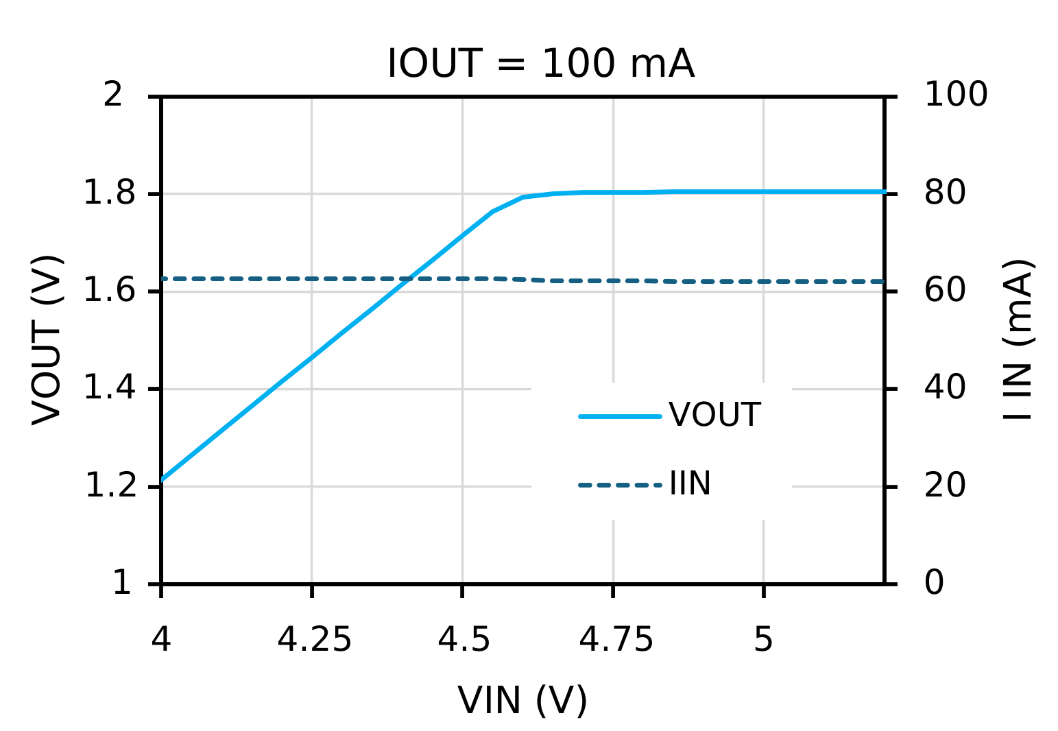
In buck ELRs, the optocouplers make use of the voltage drop between the input and output terminals of the regulator to generate usable output power—power that is wasted in a conventional linear regulator. This raises the efficiency of the linear topology significantly compared to conventional linear regulators operating over wide voltage steps. The basic principle is to use an array of LEDs in series with the LDO pass transistor to generate photons that can be captured and converted to usable output power by integrated photovoltaics. A simplified circuit topology, based on Polaris Semiconductor’s ultra-low noise BK301D18V device, is shown in Figure 1(a). The output voltage of BK30 devices is set by a single resistor, , through which a 100 µA current flows, generated by the precision current source within the LT3045 chip. The LDO minimizes the difference in the voltage across and the output voltage using a very wide bandwidth error amplifier circuit that is capable of extremely low noise and high PSRR. The set resistor is connected between the precision current source and ground, generating a voltage of 100 µA × . Over a common 5 V to 1.8 V step, this topology offers 70% higher efficiency than a conventional LDO due to a significant reduction in input current for a given output current. For example, with a 100 mA output current, BK301D18V configured with two LEDs in series draws an input current of only 61 mA (Figure 1(b)).
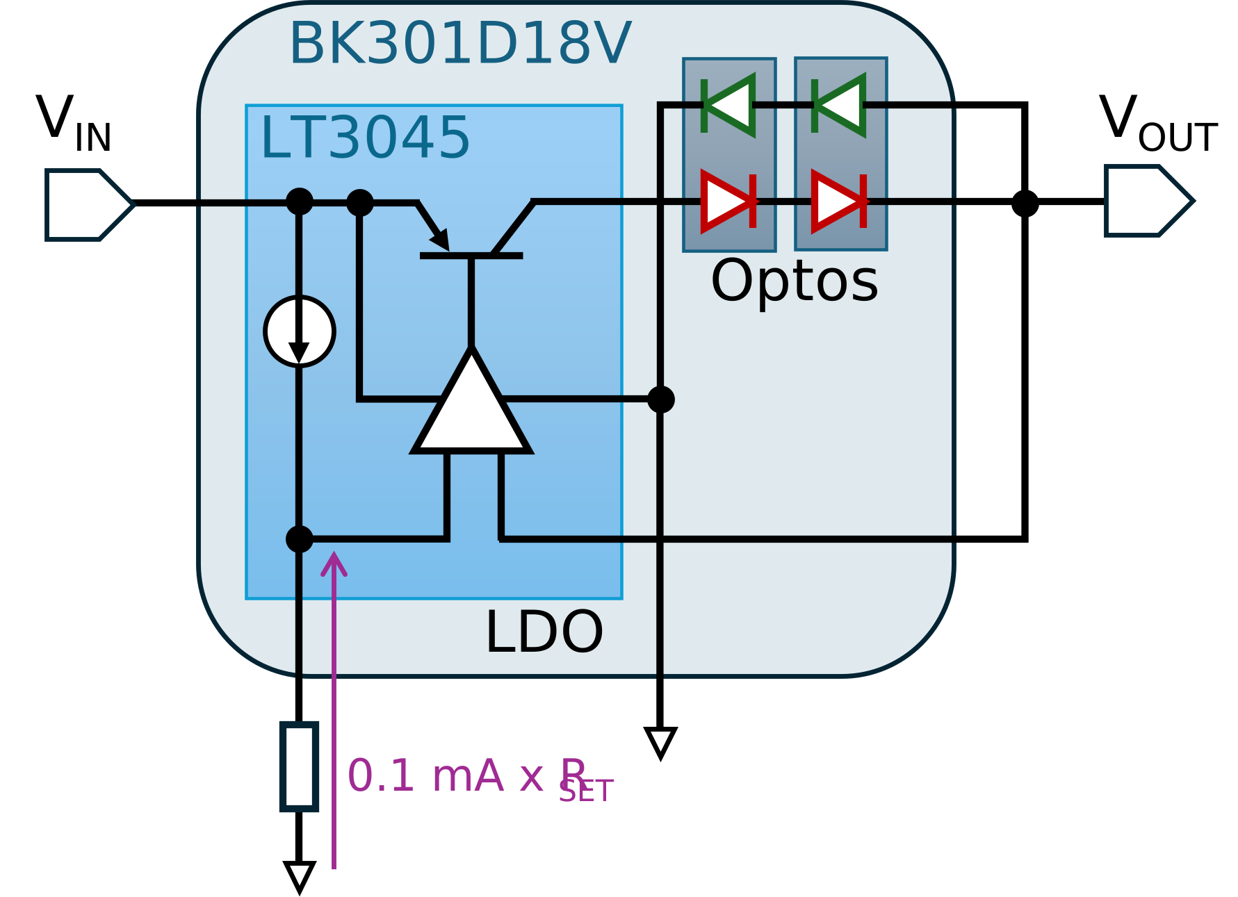
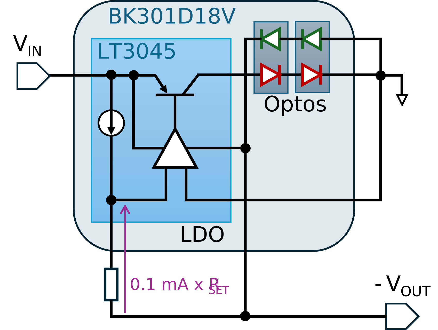
In the inverting topology, the ground reference voltage of the LDO device within the ELR is no longer referenced to the system ground, but is instead referenced to . The high side of the LED array is connected to the pass transistor of the LDO, and the low side is connected to the system ground (Figure 1(c)). The LEDs generate photocurrent in the photovoltaic array that drives a current in the load and pulls below the system ground. As before, the LDO feedback loop acts to regulate the output voltage at = −100 µA × .
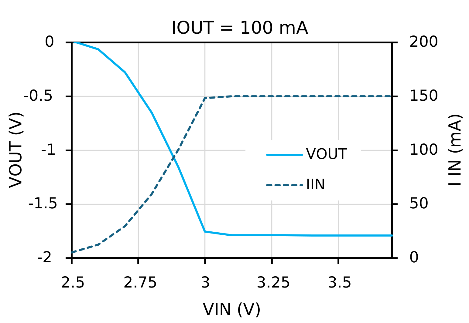
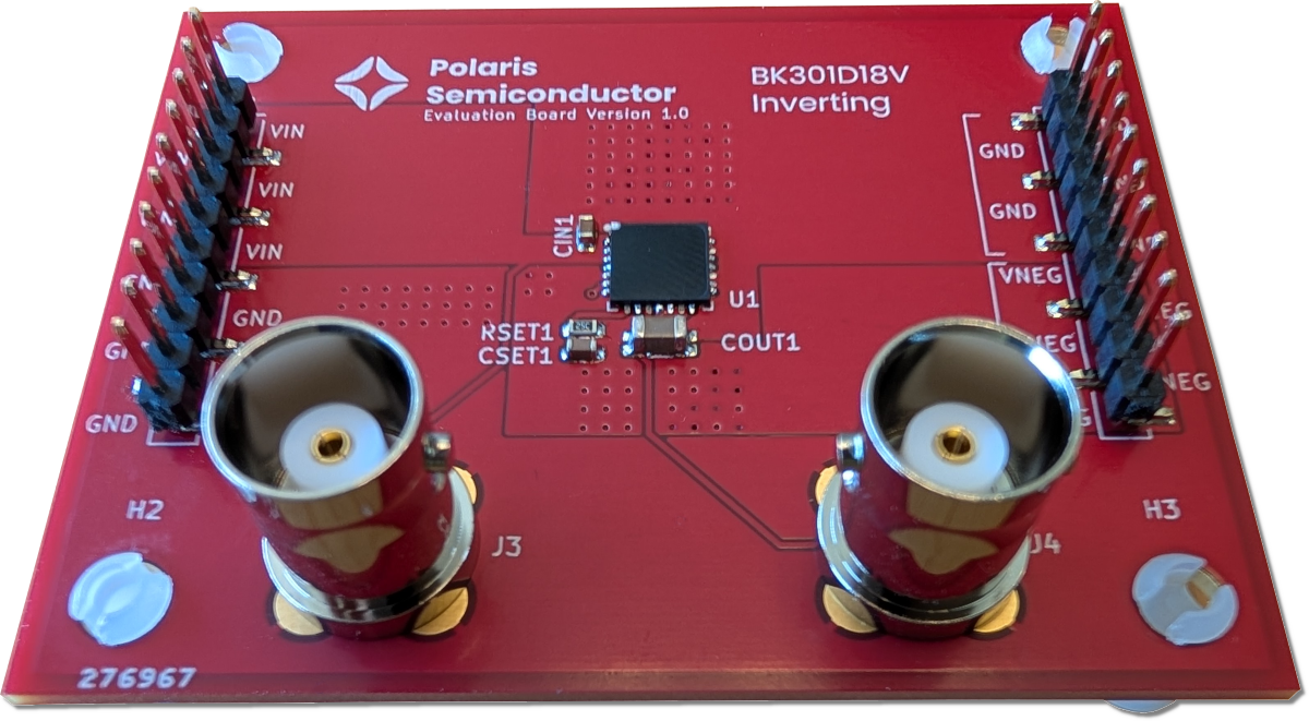
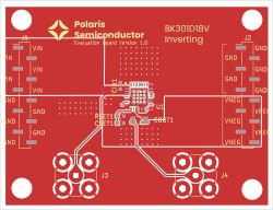
This low noise, inductor-less and switching-free inverting topology eliminates the conventional drawbacks with switching-based solutions, providing extremely low noise with a minimum of passive components. The photocurrent supplied to the load is sourced entirely from the current flowing through the LED array, and therefore the efficiency of the device is generally lower than the buck and boost topologies of ELRs, where only a fraction of output current is sourced from the optocouplers. However, in many systems, negative rails account for only a small fraction of the overall current and power budget, and therefore the efficiency penalty is largely insignificant, whereas the simplicity and noise improvements can be large. The input current draw of BK301D18V when configured for voltage inversion is greater than the output current ( = 150 mA, = 100 mA), as shown in Figure 1(d). A photograph of BK301D18V assembled on a PCB evaluation board is shown in Figure 2.
Output Current Range
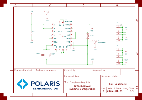
Figure 3(a) shows the input current drawn versus output current for BK301D18V with = −1.8 V and of 3.7 V and 5 V. The schematic, PCB layout and BoM is provided in the Appendix. An electronic load was used and the input current was supplied by a Keithley 2401 SMU. The board was held in ambient conditions with natural convection, and the case temperature, which is very close to the junction temperature, was measured using a FLIR thermal camera. For simplicity, we refer to the output current as a positive quantity, although the current flow is actually in the reverse direction relative to the input current.
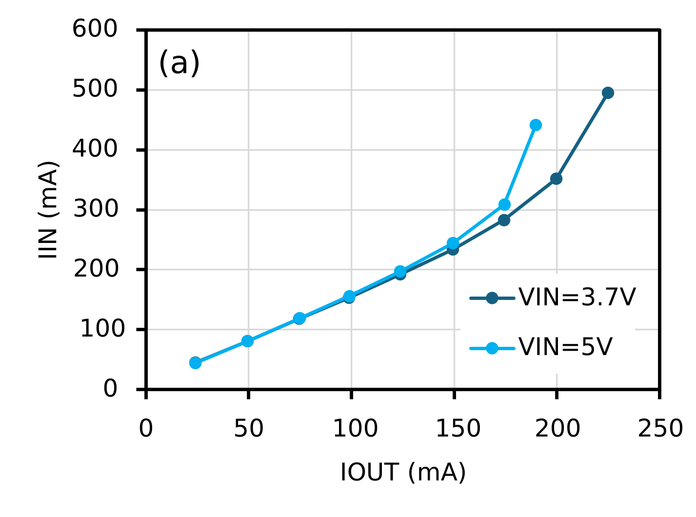
For = 3.7 V, the input current increases linearly with output current in the region of < 150 mA. In this range, the ratio of / is roughly 1.5. In the region of 150 mA to 225 mA, the temperature of the part begins to increase significantly as the dissipated power grows. The elevated temperature leads to a reduction in the efficiency of the optocouplers, combined with increased series resistance and LDO dropout losses at higher currents. These factors cause a super-linear increase in input current in this range.
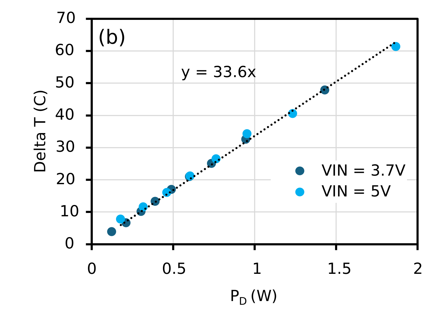
For = 5 V, the dissipated power, , increases for a given load current due to the greater voltage drop. In the region of < 150 mA, the device behavior is very similar to the case of = 3.7 V, but in the region of 150 mA to 225 mA the super-linear behavior is more pronounced than with = 3.7 V due to higher device temperatures. The maximum output current plotted in Figure 3(a) with = 5 V is 190 mA, which keeps the device temperature under 90 °C. With active cooling or heat-sinking employed, the current output of the regulator could be higher. However, the thermal resistance of the PCB, measured to be 33.6 °C/W (Figure 3(b)), places a practical limit of roughly 200 mA under the natural convection conditions in this experiment.
Ultra-low Output Noise
Polaris Semiconductor’s BK30 range of parts co-package our optocouplers with LT3045, a state-of-the-art LDO manufactured by Analog Devices that has exceptional output noise and ripple rejection performance. The output noise spectral density and integrated RMS noise was measured at Analog Devices for BK301D18V in both buck and inverting topologies. The load current was set at approximately 350 mA for the buck ELR and 200 mA for the inverting ELR using a resistive load across the output, and was 5 V. The output noise was amplified using an 80 dB low-noise amplifier [2], and the noise spectrum captured using a spectrum analyzer.
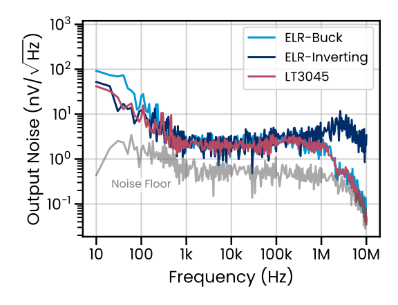
The output noise of BK301D18V configured for buck conversion with = 1.8 V was measured to be 0.96 µVRMS. This is integrated over the frequency range of 10 Hz–100 kHz. In the inverting topology, the exquisite noise performance is maintained, as shown in Figure 4(a), with an output noise magnitude of 0.89 µVRMS when configured for = −1.8 V. For comparison, an LT3045 evaluation board was measured, and the noise output of the ELRs is virtually indistinguishable from LT3045 in the 10 Hz–100 kHz range, shown in Figure 4(a). However, at frequencies above 1 MHz, the output noise of the inverting regulator is slightly higher, although still extremely low compared to inverting regulators based on switching.
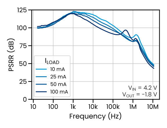
In the inverting regulator configuration, greater than 100 dB of ripple rejection over a broad frequency range is measured at a range of load currents, shown in Figure 4(b). This high performance equals the extremely high PSRR achieved in both the buck ELR and LT3045 in a standard LDO configuration.
Other ELR Arrangements
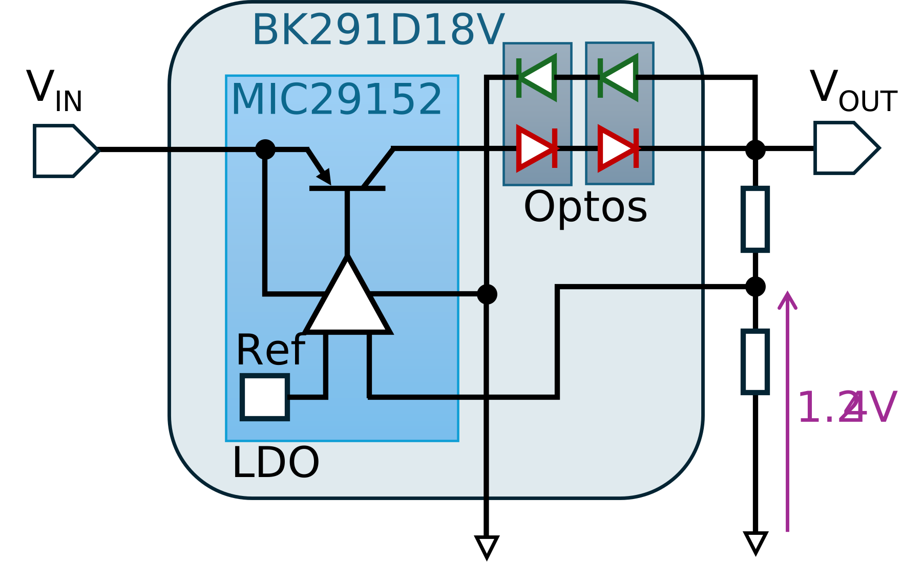
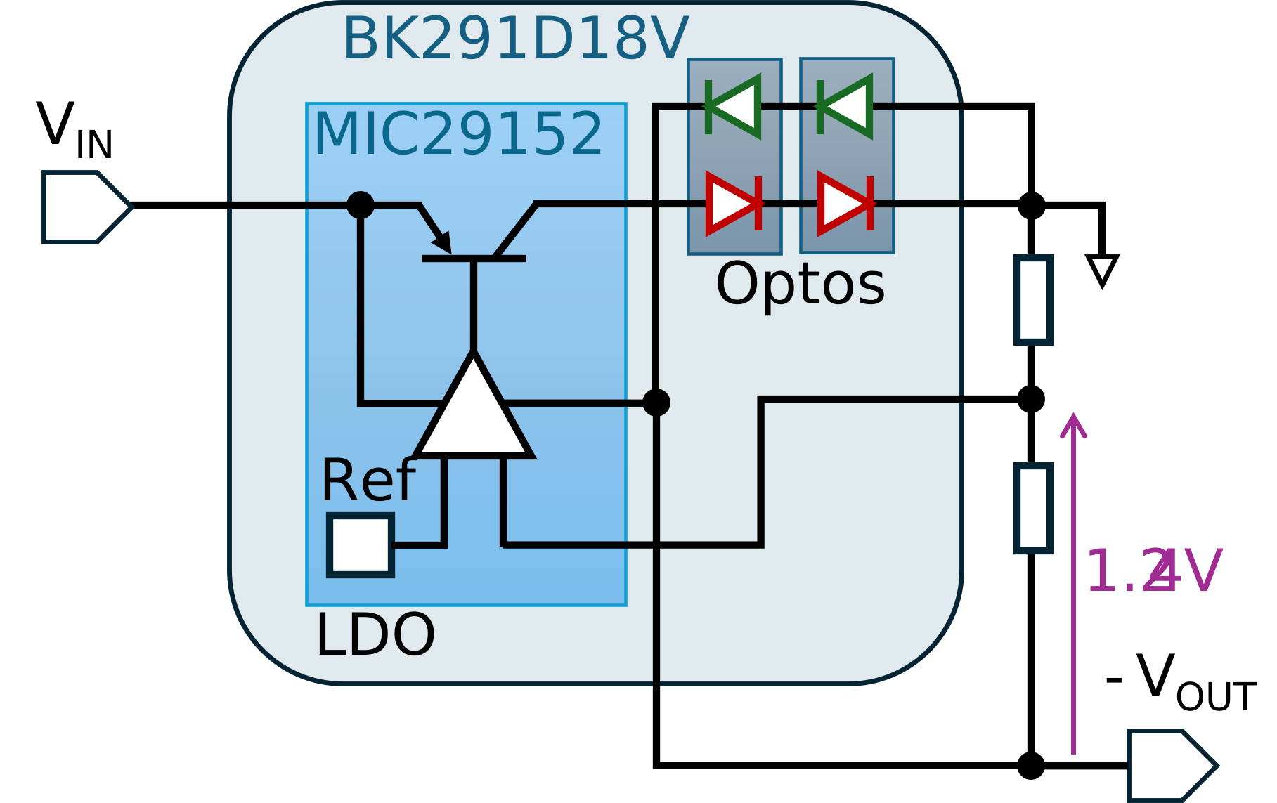
An inverting topology can be achieved with any of the buck ELR products offered by Polaris Semiconductor. For example, our general purpose, higher current BK29 ELRs can be easily configured as inverting regulators using the existing package pins. These parts use an LDO with a more conventional voltage reference scheme; a bandgap voltage reference circuit generates a reference voltage of ≈ 1.2 V which is compared to a scaled representation of via a voltage divider (Figure 5(a)). In the inverting scheme (Figure 5(b)), the ground potential of the LDO is referenced to , which is pulled below the system ground by the PV devices—analogous to the arrangement in Figure 1. This straightforward configuration allows for simple inverting and bipolar output architectures from a single supply without concerns of conducted and radiated EMI effects, and with a very low number of passives.
Conclusion
The high-efficiency optocoupler technology of Polaris Semiconductor can bring major performance enhancements to conventional linear regulators, such as high efficiency buck conversion over wide voltage steps and efficient switching-free boost conversion. In this application note, we show how the pin connections of ELR devices can be configured in a way that turns a device from a buck regulator into an inverting regulator, generating a regulated negative voltage from a positive supply. Using our BK30 series of devices, built using Analog Devices’ LT3045 technology, we demonstrate inverting regulator integrated output noise below 1 µVRMS and ripple rejection above 100 dB with a compact footprint and low component count.
Appendix
BK301D18V Inverting Regulator Schematic
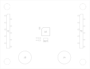
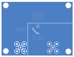
BK301D18V Inverting Regulator PCB Layout
BK301D18V Inverting Regulator Bill of Materials
| ID | Description | Part | Manufacturer |
|---|---|---|---|
| CIN1, CSET1 | 4.7 µF 16 V ceramic X7R 0603 | GRM188Z71C475KE21J | Murata Electronics |
| COUT1 | 10 µF 50 V ceramic X7R 1206 | CL31B106KBHNNNE | Samsung Electro-Mechanics |
| RSET1 | 17.8 kΩ 0.1% 1/10 W 0603 | RG1608P-1782-B-T5 | Susumu |
| J1, J2 | Header, 2.54 mm pitch, 40 positions, surface mount | HDR100IMP40M-G-V-SM | Chip Quik Inc. |
| J3, J4 | BNC jack, 50 Ω, through hole | CONBNC001 | TE Connectivity Linx |
| U1 | Enhanced Linear Regulator (ELR) | BK301D18V | Polaris Semiconductor |
References
- LT3045 20V, 500mA, ultralow noise, ultrahigh PSRR linear regulator. Analog Devices; Datasheet, 2022. Available: https://www.analog.com/media/en/technical-documentation/data-sheets/lt3045.pdf
- T. Owen and A. Patel, “Measuring 2nV/√Hz noise and 120dB supply rejection on linear regulators.” Linear Technology (now Analog Devices); Application Note AN-159, 2016. Available: https://www.analog.com/en/resources/app-notes/an-159.html
Ready to design it in?
Request evaluation samples, detailed datasheets, and SPICE models — an engineer answers, not a sales funnel.